Ultra-low power design strategy for two-stage amplifier topologies
Lieuwe B. Leene, Timothy G. Constandinou
Department of Electrical and Electronic Engineering, Imperial College London, SW7 2BT, UK
Centre for Bio-Inspired Technology, Institute of Biomedical Engineering, Imperial College London, SW7 2AZ, UK
Abstract
This letter presents a novel two stage amplifier topology and ultra low power design strategy for two stage amplifiers that utilises pole zero cancellation to address the additional power requirements for stability. For a 288nA total bias, the presented amplifier achieves a 1.07 MHz unity gain frequency with a 8560 pF MHz/mA figure of merit.
1 Introduction
Power efficient amplifier topologies are fundamental analogue processing both in the continuous and discrete time domains. The feasibility of a system is often established using a relevant figure of merit (FOM) that quantifies performance. The prevalence of limited power budgets in medical sensors indicates that advances in low power analogue are critical for the future of implantable biomedical systems that are constrained through battery life and wireless telemetry 1 2. Ultra low power analogue design is best motivated through aggressively maximising a FOM that indicates how effectively power is used to achieve a desired performance characteristic such as noise, speed, or linearity in order to reveal the underlying limitation.
Taking the differential pair in Fig. 1 for example to illustrate the driving motivation behind sub-threshold operation. The FOM with all transistors in strong inversion can reduced to a single operational parameter;
$$ FOM_{si} \left[ \frac{pF \cdot MHz} {mA} \right] = \frac{UGF \cdot C_{L}}{I_{total}} = \frac{10^{3}}{2 \pi V_{ov}} $$
Where \(UGF\), \(C_{L}\), \(I_{total}\), and \(V_{ov}\) are the unity gain frequency, load capacitance, total bias current, and over drive voltage of the input transistors respectively. With the input transistors biased in weak inversion however the FOM is derived as;
$$ FOM_{wi} = \frac{10^{3}}{4 \pi \cdot \eta U_{T}} $$
With \(\eta\) & \(U_{T}\) being the sub-threshold slope factor and thermal voltage respectively. With \(V_{ov}\) usually being 200mV, operation in weak inversion can directly improve the FOM by 6 times. In addition to sub-threshold biasing a number of current recycling techniques can be applied to further gain in FOM 3. By coupling the input signal to biasing transistors \(M_{3-4}\) for instance, a larger transconductance can be achieved with the same bias current. This allows a simple reduction in power by a factor of two for single stage systems, but a second stage is often required in switched capacitor (SC) applications for high gain and wide output swing. The constraint of the second stage lies with the non-dominant pole at the output that needs to lie beyond the unity gain frequency. The output load capacitance dictates the minimum transconductance of the second stage and will often result in the second stage dissipating significantly more power than the first stage. In this letter, we propose zero cancellation of this non-dominant pole in order to minimise power dissipation in the second stage. Secondly, we identify appropriate scaling factors for the FOM such as to make this applicable to two stage amplifiers.
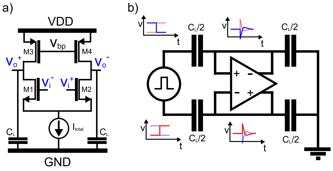
Figure 1: circuit schematics for: (a) simple differential pair with differential output; (b) unity feedback configuration used for testing the transient step response of a fully differential amplifier.
2 Proposed amplifier
The circuit configuration is shown in Fig. 2. This differential topology extends the complementary input stage with a current conveyor (CC) structure to achieve high gain and wide output swing. The high open loop gain is provided by the cross coupled PMOS devices \(M_{11-14}\) in addition to the traditional gain stage \(M_{19-22}\) that also allows for a rail to rail output swing. The circuit is configured to drain the same amount of current in the output branch as in the input transistor pair such that the transistors \(M_{1-6}\) & \(M_{19-22}\) have a transconductance \(gm_{1}\). The cross coupled PMOS branch drains a fraction (1/M = 0.25) of this same current such that the total current dissipated by the amplifier is \(2I_{M1} \cdot (2 + 1/M)\). The NMOS current mirror \(M_{15-18}\) implements a wideband positive feedback loop with a ratio of 1:N-1 where N = 1.5 to boost the bandwidth of the structure. Note that transistors \(M_{23-24}\) bias the input stage through common mode feedback and transistors \(M_{7-10}\) bias the output stage. The input transistors \(M_{1-6}\) are biased with a drain current \(I_{input}\) of 50nA with a 1.2V supply. This biasing current in addition to the ratio \(M\) determine the observed single ended slew rate (SR) at the output as it is limited by the low gain path in the NMOS current mirror. In the step response scenario the current drained by \(M_{23}\) sources entirely into \(M_{15}\) \(M_{18}\) which is multiplied to \(M_{19}\) \(M_{20}\) by a factor \(M\), that is;
$$ SR = M \cdot \frac{2 I_{input}}{C_{L}} $$
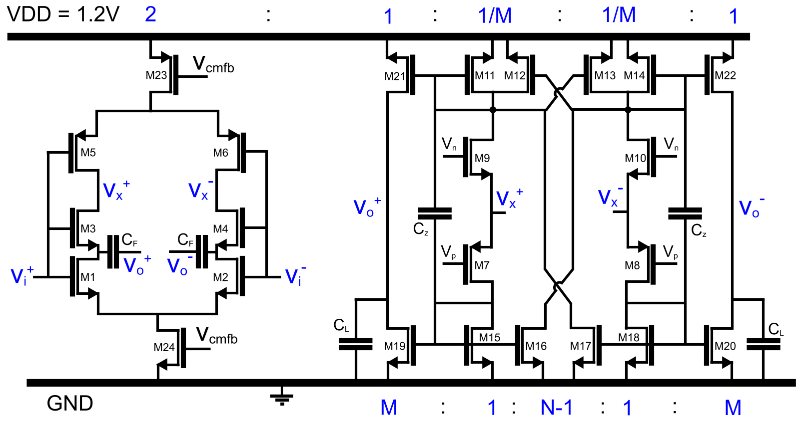
Figure 2: Circuit schematic of the proposed amplifier topology including the input stage (on left) and CC stage (on right). Vp & Vn are externally provided DC biasing voltages.
For preliminary design considerations it is useful to assess the dependence of different component parameters through the open loop gain, unity gain frequency, pole and zero locations with simple approximations. First it should be noted the bandwidth product is twice as large as a conventional amplifier though current recycling in the complementary input transistor pairs and evaluated as;
$$ UGF = \frac{gm_{1} }{ \pi \cdot C_{F}} $$
Where \(C_{F}\) is a 500 fF compensation capacitor that couples the output to the input stage via a low impedance node in the NMOS differential pair utilising split length indirect compensation, thus avoiding the right hand plane pole 4. With \(\lambda\) as the channel length modulation parameter the open loop DC gain is evaluated as;
$$ A_{dc} \approx NM \left( \frac{1}{\eta U_{T} \lambda} \right)^{2} $$
Furthermore in the midband frequencies the Miller capacitor \(C_{F}\) performs pole splitting both poles in the CC stage through the feedback loop. This will move the pole at the cross coupled PMOS outside the UGF, more specifically \(\omega_{p2}\), and move the pole due to \(C_{L}\) towards;
$$ \omega_{p1} \approx \frac{2M \cdot gm_{1}}{C_{L} + C_{z}} $$
If \(gm_{1}\) is kept small this pole will remain in-band of the amplifier. For adequate phase margin that is larger than \(65^{\circ}\), to prevent excess ringing at the output, we use pole zero cancellation. With \(\omega_{p1} = \omega_{z}\), \(C_{z}\) is determined according to;
$$ \omega_{z} \approx \frac{gm_{M15} \cdot (2-N)}{ C_{z}} $$
\noindent Past the zero location, the signal path loads into the diode-connected NMOS \(M_{15}\) that now drives both \(M_{21}\) & \(M_{19}\) pushing out the unity gain frequency. With \(C_{gs}\) as the total gate capacitance from both NMOS & PMOS current mirrors and taking \(C_{z}\) as a short circuit, the pole location \(\omega_{p2}\) can be confirmed to lie outside the unity gain frequency;
$$ \omega_{p2} \approx \frac{2 gm_{1}}{C_{gs}} $$
$$ FOM \approx \frac{10^{3}}{4 \pi \cdot \eta U_{T}} \cdot \frac{2 \cdot C_{F}/C_{L}}{2 + 1/M} = 3.56 \times FOM_{wi} $$
As a result, when the FOM is reformulated (see above) for this particular configuration, it can be observed that this is increased, compared to the conventional single stage topology. A significant contribution of this improvement in FOM naturally comes from the factor \(C_{F}/C_{L}\) as a reduction in the dominant capacitive load allows a overall reduction in bias current to achieve a given bandwidth. This also illustrates that relative to a single stage, a two stage configuration may trade off noise for a better FOM by adjusting the \(C_{F}/C_{L}\) ratio. As the total input referred integrated thermal noise \(e^{2}_{in}\) for a single pole system is related to the capacitor \(C\) that introduces the dominant pole of the system through:
$$ e^2 = \frac{ kT }{C} \frac{ kT NEF^{2} \cdot I_{input}}{ \eta A_{cl} I_{total} } $$
Which is directly derived from the definition of the noise efficiency factor (NEF) 5 by substituting the expression for bandwidth as the closed loop gain \(A_{cl}\) multiplied by UGF.
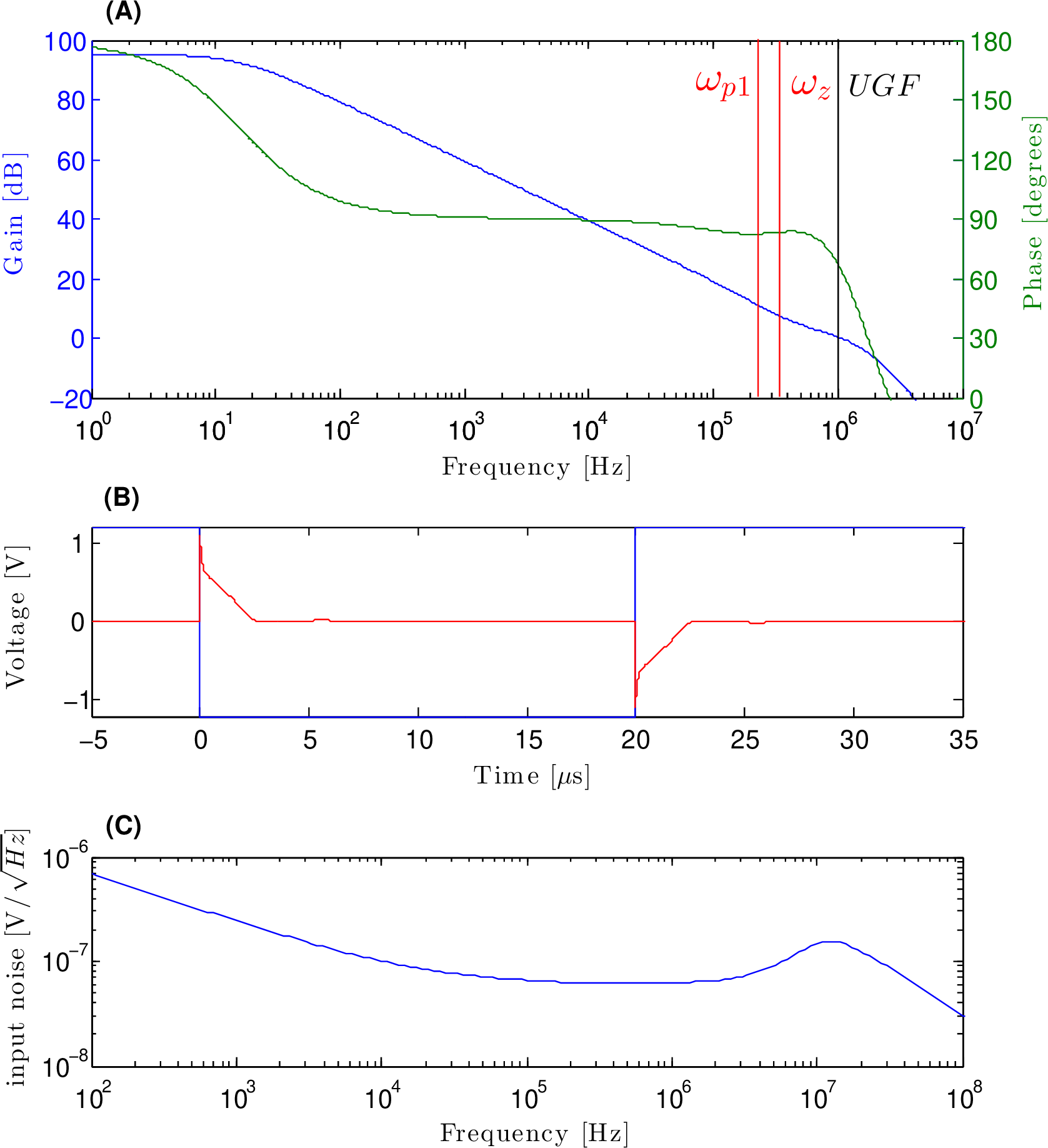
Figure 3: Simulation Results: (a) open loop frequency response (b) closed loop step response of differential signals (c) input referred noise density.
Table 1: Performance Summary
| Reference | 6 | 7 | 4 | This work |
|---|---|---|---|---|
| Year | 2009 | 2010 | 2010 | 2013 |
| Tech. [nm] | 180 | 180 | 500 | 180 |
| Power [W] | 5.5m | 600μ | 1.2m | 345n |
| Supply Voltage [V] | 1.2 | 1.5 | 3 | 1.2 |
| DC Gain [dB] | 85 | 59 | 82 | 96 |
| UGF [MHz] | 450 | 111 | 20 | 1.07 |
| Slew Rate [V/μs] | - | 233 | 8 | 0.12 |
| Load/Miller [pF] | -/3 | 5 | 5, 0.2/500 | 2/0.5 |
| Phase Margin [°] | 68 | 80 | 72 | 64 |
| Noise Floor [V/√Hz] | - | 125n | - | 60n |
| FOM [MHz pF/mA] | 295 | 1267 | 8333 | 8560 |
3 Simulation Results
Preliminary validation of the proposed implementation has been achieved using schematic level simulations in the Cadence IC 6.1.5 Design Environment using industry provided transistor models for the commercially available 6 Metal 0.18 μm CMOS technology (AMS/IBM C18A6/7SF). Fig. 3 shows key simulation results, including small signal, transient, and noise characteristics. The common mode feedback configuration used in these simulations is a conventional differential difference amplifier with a current mirror to drive both M23 & M24 transistors biasing the input stage simultaneously. In order to normalise performance with respect to requirements on the common mode feedback circuit its 45nW power contribution is excluded in FOM calculations. The simulated frequency characteristics were close to the analytical expectation achieving a 1.07MHz unity gain frequency and a phase margin of 64 degrees. The step response indicates settling of the output to <0.1 % within 10 μs with the feedback configuration illustrated in Fig. 1. The configuration also demonstrates good noise performance as the input transistors have a larger transconductance than the first active load by a factor of M for a smaller input referred noise figure. The 60 nV/√Hz input referred thermal noise floor from 100kHz to 1MHz is good for auto zeroing SC topologies that rejects the flicker noise and low frequency aggressors.
4 Conclusion
The application of pole zero cancellation for achieving ultra low power in two stage amplifier has been demonstrated. In addition the Miller to load capacitor ratio and current recycling have been discussed as techniques to improve the FOM with the respective trade off. The overall performance characteristics are summarized in table 1. This demonstrates comparable performance to state of the art three stage nested miller systems in terms of FOM in addition to a 345nW power budget that is well within the power constraints of many biomedical analogue processing applications. The proposed topology achieves a 3.56 times improvement in FOM over conventional single stage structures.
5 Acknowledgment
This work was supported by the UK EPSRC (grants EP/I000569/1 and EP/K015060/1).
Refernces:
A.Eftekhar, E.P. Sivylla, and G.C. Timothy, ‘‘Towards a next generation neural interface: Optimizing power, bandwidth and data quality,’’ in IEEE Proc. BIOCAS, 2010, pp. 122–125. ↩︎
W.Wattanapanitch and R.Sarpeshkar, ‘‘A low-power 32-channel digitally programmable neural recording integrated circuit,’’ IEEE Trans. Biomed. Circuits Syst., vol.5, no.6, pp. 592–602, 2011. ↩︎
R.Assaad and J.Silva-Martinez, ‘‘Enhancing general performance of folded cascode amplifier by recycling current,’’ IET Elec. Letters, vol.43, no.23, 2007. ↩︎
V.Saxena and R.J. Baker, ‘‘Indirect compensation techniques for three-stage fully-differential op-amps,’’ in IEEE Proc. MWSCAS, 2010, pp. 588–591. ↩︎ ↩︎
R.Harrison and C.Charles, ‘‘A low-power low-noise cmos amplifier for neural recording applications,’’ IEEE J. Solid-State Circuits, vol.38, no.6, pp. 958–965, 2003. ↩︎
M.Fan, J.Ren, Y.Guo, Y.Li, N.Li, F.Ye, and J.Xu, ‘‘Low-voltage low-power operational amplifier for sc circuits,’’ IET Elec. Letters, vol.45, no.25, pp. 1274–1276, 2009. ↩︎
M.Yavari, ‘‘Single-stage class ab operational amplifier for sc circuits,’’ IET Elec. Letters, vol.46, no.14, pp. 977–979, 2010. ↩︎